Search a title or topic

Over 20 million podcasts, powered by 

Player FM logo
Artwork

Content provided by Dave Jones & Chris Gammell, Dave Jones, and Chris Gammell. All podcast content including episodes, graphics, and podcast descriptions are uploaded and provided directly by Dave Jones & Chris Gammell, Dave Jones, and Chris Gammell or their podcast platform partner. If you believe someone is using your copyrighted work without your permission, you can follow the process outlined here https://podcastplayer.com/legal.
Player FM - Podcast App
Go offline with the Player FM app!

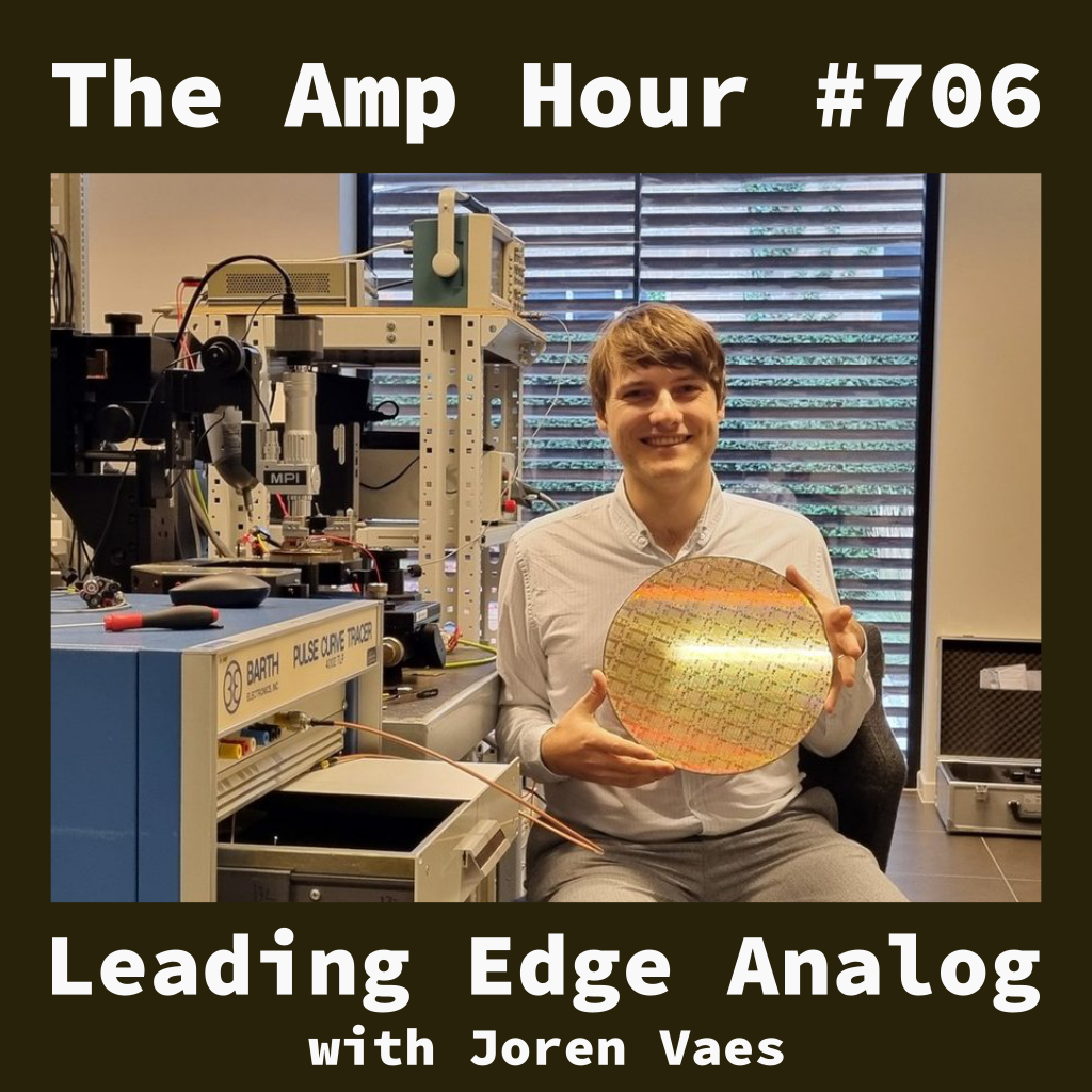
#706 – Leading Edge Analog with Joren Vaes

1:04:25
 
Share
 

Manage episode 514443384 series 2133
Content provided by Dave Jones & Chris Gammell, Dave Jones, and Chris Gammell. All podcast content including episodes, graphics, and podcast descriptions are uploaded and provided directly by Dave Jones & Chris Gammell, Dave Jones, and Chris Gammell or their podcast platform partner. If you believe someone is using your copyrighted work without your permission, you can follow the process outlined here https://podcastplayer.com/legal.

Welcome Joren Vaes, design engineer at SOFICS

  • Simulation is critical when designing analog devices based on a PDK from the fab
  • Parasitics are significant, especially with new nodes having upwards of 16 metal layers
  • Chris complained about a class where the professor made them draw planar structures with graph paper with colored pencils
  • Large fabs on leading edge nodes have 1800 page textbook of rules
  • Because the constraints get tighter, that book gets longer for each node
  • 2 nm mass production on finfet currently with TSMC
  • 22 was the last classic cmos
  • Finfet, looks like a devil
  • ‘gate all around’ / nanosheet
  • CFET (complementary field effect transistor) is next
  • Joren really gets Maxwells Equations…as you have to at super high speeds
  • SOFICS are making phy’s / IP blocks
  • Amplifiers that are DC to 50 GHz
  • Making a datasheet for the resulting IP block
  • Joren got his PhD working on millimeter wave applications
  • It’s all just physics
  • Using coils to impedance match between layers
  • Reflecting off of different materials at angles is Snells law (not lorentz equation) and that extends to different materials at different wavelengths
  • Cables are very lossy at 100 GHz…dBs per cm
  • Parasitics impact every part of the design process
  • Wireline community – name for the high speed interfaces, including research in the space
  • Most transistor threshhold voltages that Joren works with are … 750 mV!
  • Voltage dependent drc rules
  • Electromigration – holes in wires from electrons
  • ESD is a big part of the business, and a large source of parasitics
  • New product development for IP blocks
  • Working with customers and Foundry at the 2 nm node
  • Design companies need to be paying 100s of thousands to software providers
  • After, it goes to spice and schedmatic
  • Joren decides whether to jump in on layout
  • LVS – layout vs schematic
  • Parasitic extraction (spice netlist)
  • PDKs define how you can do the layout stage
  • Lower cost tools exist but more expensive tools have tooling that tells you when you’re violating DRC
  • 3 main vendors
    • Cadence
    • Synopsis
    • Siemens (Caliber)
  • Foundries soemtimes only support one tool
  • Doing test wafers allows testing of structures. They often get MPW at a discount from the fab (since they’re often testing new processes as well)
  • How do they test with packaging options?
    • ‘low speed’ can be die bonded or pcb mounted
    • high speed does on wafer probing (with veeeery expensive probes)
  • Check out Sofics.com for more info on the company. They also have a blog with a great name.
  • Follow or connect with Joren on LinkedIn

  continue reading

307 episodes

Artwork
iconShare
 
Manage episode 514443384 series 2133
Content provided by Dave Jones & Chris Gammell, Dave Jones, and Chris Gammell. All podcast content including episodes, graphics, and podcast descriptions are uploaded and provided directly by Dave Jones & Chris Gammell, Dave Jones, and Chris Gammell or their podcast platform partner. If you believe someone is using your copyrighted work without your permission, you can follow the process outlined here https://podcastplayer.com/legal.

Welcome Joren Vaes, design engineer at SOFICS

  • Simulation is critical when designing analog devices based on a PDK from the fab
  • Parasitics are significant, especially with new nodes having upwards of 16 metal layers
  • Chris complained about a class where the professor made them draw planar structures with graph paper with colored pencils
  • Large fabs on leading edge nodes have 1800 page textbook of rules
  • Because the constraints get tighter, that book gets longer for each node
  • 2 nm mass production on finfet currently with TSMC
  • 22 was the last classic cmos
  • Finfet, looks like a devil
  • ‘gate all around’ / nanosheet
  • CFET (complementary field effect transistor) is next
  • Joren really gets Maxwells Equations…as you have to at super high speeds
  • SOFICS are making phy’s / IP blocks
  • Amplifiers that are DC to 50 GHz
  • Making a datasheet for the resulting IP block
  • Joren got his PhD working on millimeter wave applications
  • It’s all just physics
  • Using coils to impedance match between layers
  • Reflecting off of different materials at angles is Snells law (not lorentz equation) and that extends to different materials at different wavelengths
  • Cables are very lossy at 100 GHz…dBs per cm
  • Parasitics impact every part of the design process
  • Wireline community – name for the high speed interfaces, including research in the space
  • Most transistor threshhold voltages that Joren works with are … 750 mV!
  • Voltage dependent drc rules
  • Electromigration – holes in wires from electrons
  • ESD is a big part of the business, and a large source of parasitics
  • New product development for IP blocks
  • Working with customers and Foundry at the 2 nm node
  • Design companies need to be paying 100s of thousands to software providers
  • After, it goes to spice and schedmatic
  • Joren decides whether to jump in on layout
  • LVS – layout vs schematic
  • Parasitic extraction (spice netlist)
  • PDKs define how you can do the layout stage
  • Lower cost tools exist but more expensive tools have tooling that tells you when you’re violating DRC
  • 3 main vendors
    • Cadence
    • Synopsis
    • Siemens (Caliber)
  • Foundries soemtimes only support one tool
  • Doing test wafers allows testing of structures. They often get MPW at a discount from the fab (since they’re often testing new processes as well)
  • How do they test with packaging options?
    • ‘low speed’ can be die bonded or pcb mounted
    • high speed does on wafer probing (with veeeery expensive probes)
  • Check out Sofics.com for more info on the company. They also have a blog with a great name.
  • Follow or connect with Joren on LinkedIn

  continue reading

307 episodes

All episodes

×
 
Loading …

Welcome to Player FM!

Player FM is scanning the web for high-quality podcasts for you to enjoy right now. It's the best podcast app and works on Android, iPhone, and the web. Signup to sync subscriptions across devices.


Copyright 2025 | Privacy Policy | Terms of Service | | Copyright
Listen to this show while you explore
Play