Flash Forward is a show about possible (and not so possible) future scenarios. What would the warranty on a sex robot look like? How would diplomacy work if we couldn’t lie? Could there ever be a fecal transplant black market? (Complicated, it wouldn’t, and yes, respectively, in case you’re curious.) Hosted and produced by award winning science journalist Rose Eveleth, each episode combines audio drama and journalism to go deep on potential tomorrows, and uncovers what those futures might re ...
…
continue reading
Content provided by The Amp Hour (Chris Gammell and David L Jones), The Amp Hour (Chris Gammell, and David L Jones). All podcast content including episodes, graphics, and podcast descriptions are uploaded and provided directly by The Amp Hour (Chris Gammell and David L Jones), The Amp Hour (Chris Gammell, and David L Jones) or their podcast platform partner. If you believe someone is using your copyrighted work without your permission, you can follow the process outlined here https://podcastplayer.com/legal.
Similar to The Amp Hour Electronics Podcast
A myriad of AI, science, and technology experts explore the real challenges and enormous opportunities facing entrepreneurs who are building the future of health. Raising Health, a podcast by a16z Bio + Health and hosted by Kris Tatiossian and Olivia Webb, dives deep into the heart of biotechnology and healthcare innovation. Join veteran company builders, operators, and investors Vijay Pande, Julie Yoo, Vineeta Agarwala, and Jorge Conde, along with distinguished guests like Mark Cuban, Greg ...
…
continue reading
DNA science. Artificial intelligence. Smartphones and 3D printers. Science and technology have transformed the world we live in. But how did we get here? It wasn’t by accident. Well, sometimes it was. It was also the result of hard work, teamwork, and competition. And incredibly surprising moments. Hosted by bestselling author Steven Johnson (“How We Got To Now”), American Innovations uses immersive scenes to tell the stories of the scientists, engineers, and ordinary people behind the great ...
…
continue reading
When you hear the words Alzheimer's disease, what do you think of? The truth is, the picture most of us have of the disease is incomplete. Alzheimer's disease doesn't start when someone starts to lose their memory. It actually starts years – sometimes decades – earlier. The Rethinking Alzheimer's Disease Podcast is an engaging, narrative-style podcast miniseries for those curious or motivated to learn about Alzheimer’s disease. Perhaps you have a family member with Alzheimer’s disease, or ca ...
…
continue reading
Scientists Daniel and Kelly cannot stop talking about our amazing, wonderful, weird Universe! Each episode is a fun, easy-to-understand, and in-depth explanation of topics in science, from particles to black holes to moon colonies to ecosystems to parasites and everything else in the Universe!
…
continue reading
Hanselminutes is Fresh Air for Developers. A weekly commute-time podcast that promotes fresh technology and fresh voices. Talk and Tech for Developers, Life-long Learners, and Technologists.
…
continue reading
Whether the topic is popcorn or particle physics, you can count on BrainStuff to explore -- and explain -- the everyday science in the world around us.
…
continue reading
The surprising connections in science and technology that give you the Big Picture. Astronomer Seth Shostak and science journalist Molly Bentley are joined each week by leading researchers, techies, and journalists to provide a smart and humorous take on science. Our regular "Skeptic Check" episodes cast a critical eye on pseudoscience.
…
continue reading
We humans could have a bright future ahead of us that lasts billions of years. But we have to survive the next 200 years first. Join Josh Clark of Stuff You Should Know for a 10-episode deep dive that explores the future of humanity and finds dangers we have never encountered before lurking just ahead. And if we humans are alone in the universe, if we don't survive intelligent life dies out with us too.
…
continue reading
1
Sean Carroll's Mindscape: Science, Society, Philosophy, Culture, Arts, and Ideas
Sean Carroll | Wondery
Ever wanted to know how music affects your brain, what quantum mechanics really is, or how black holes work? Do you wonder why you get emotional each time you see a certain movie, or how on earth video games are designed? Then you’ve come to the right place. Each week, Sean Carroll will host conversations with some of the most interesting thinkers in the world. From neuroscientists and engineers to authors and television producers, Sean and his guests talk about the biggest ideas in science, ...
…
continue reading
Player FM - Podcast App
Go offline with the Player FM app!
Go offline with the Player FM app!

))
#706 – Leading Edge Analog with Joren Vaes
Manage episode 514455203 series 2460988
Content provided by The Amp Hour (Chris Gammell and David L Jones), The Amp Hour (Chris Gammell, and David L Jones). All podcast content including episodes, graphics, and podcast descriptions are uploaded and provided directly by The Amp Hour (Chris Gammell and David L Jones), The Amp Hour (Chris Gammell, and David L Jones) or their podcast platform partner. If you believe someone is using your copyrighted work without your permission, you can follow the process outlined here https://podcastplayer.com/legal.
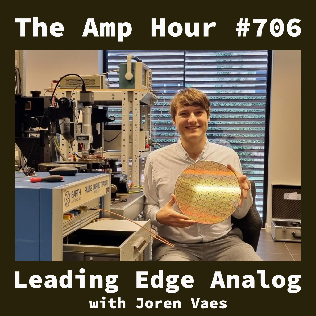
Welcome Joren Vaes, design engineer at SOFICS
- Simulation is critical when designing analog devices based on a PDK from the fab
- Parasitics are significant, especially with new nodes having upwards of 16 metal layers
- Chris complained about a class where the professor made them draw planar structures with graph paper with colored pencils
- Large fabs on leading edge nodes have 1800 page textbook of rules
- Because the constraints get tighter, that book gets longer for each node
- 2 nm mass production on finfet currently with TSMC
- 22 was the last classic cmos
- Finfet, looks like a devil
- ‘gate all around’ / nanosheet
- CFET (complementary field effect transistor) is next
- Joren really gets Maxwells Equations…as you have to at super high speeds
- SOFICS are making phy’s / IP blocks
- Amplifiers that are DC to 50 GHz
- Making a datasheet for the resulting IP block
- Joren got his PhD working on millimeter wave applications
- It’s all just physics
- Using coils to impedance match between layers
- Reflecting off of different materials at angles is Snells law (not lorentz equation) and that extends to different materials at different wavelengths
- Cables are very lossy at 100 GHz…dBs per cm
- Parasitics impact every part of the design process
- Wireline community – name for the high speed interfaces, including research in the space
- Most transistor threshhold voltages that Joren works with are … 750 mV!
- Voltage dependent drc rules
- Electromigration – holes in wires from electrons
- ESD is a big part of the business, and a large source of parasitics
- New product development for IP blocks
- Working with customers and Foundry at the 2 nm node
- Design companies need to be paying 100s of thousands to software providers
- After, it goes to spice and schedmatic
- Joren decides whether to jump in on layout
- LVS – layout vs schematic
- Parasitic extraction (spice netlist)
- PDKs define how you can do the layout stage
- Lower cost tools exist but more expensive tools have tooling that tells you when you’re violating DRC
- 3 main vendors
- Cadence
- Synopsis
- Siemens (Caliber)
- Foundries soemtimes only support one tool
- Doing test wafers allows testing of structures. They often get MPW at a discount from the fab (since they’re often testing new processes as well)
- How do they test with packaging options?
- ‘low speed’ can be die bonded or pcb mounted
- high speed does on wafer probing (with veeeery expensive probes)
- Check out Sofics.com for more info on the company. They also have a blog with a great name.
- Follow or connect with Joren on LinkedIn
61 episodes
Manage episode 514455203 series 2460988
Content provided by The Amp Hour (Chris Gammell and David L Jones), The Amp Hour (Chris Gammell, and David L Jones). All podcast content including episodes, graphics, and podcast descriptions are uploaded and provided directly by The Amp Hour (Chris Gammell and David L Jones), The Amp Hour (Chris Gammell, and David L Jones) or their podcast platform partner. If you believe someone is using your copyrighted work without your permission, you can follow the process outlined here https://podcastplayer.com/legal.
Welcome Joren Vaes, design engineer at SOFICS
- Simulation is critical when designing analog devices based on a PDK from the fab
- Parasitics are significant, especially with new nodes having upwards of 16 metal layers
- Chris complained about a class where the professor made them draw planar structures with graph paper with colored pencils
- Large fabs on leading edge nodes have 1800 page textbook of rules
- Because the constraints get tighter, that book gets longer for each node
- 2 nm mass production on finfet currently with TSMC
- 22 was the last classic cmos
- Finfet, looks like a devil
- ‘gate all around’ / nanosheet
- CFET (complementary field effect transistor) is next
- Joren really gets Maxwells Equations…as you have to at super high speeds
- SOFICS are making phy’s / IP blocks
- Amplifiers that are DC to 50 GHz
- Making a datasheet for the resulting IP block
- Joren got his PhD working on millimeter wave applications
- It’s all just physics
- Using coils to impedance match between layers
- Reflecting off of different materials at angles is Snells law (not lorentz equation) and that extends to different materials at different wavelengths
- Cables are very lossy at 100 GHz…dBs per cm
- Parasitics impact every part of the design process
- Wireline community – name for the high speed interfaces, including research in the space
- Most transistor threshhold voltages that Joren works with are … 750 mV!
- Voltage dependent drc rules
- Electromigration – holes in wires from electrons
- ESD is a big part of the business, and a large source of parasitics
- New product development for IP blocks
- Working with customers and Foundry at the 2 nm node
- Design companies need to be paying 100s of thousands to software providers
- After, it goes to spice and schedmatic
- Joren decides whether to jump in on layout
- LVS – layout vs schematic
- Parasitic extraction (spice netlist)
- PDKs define how you can do the layout stage
- Lower cost tools exist but more expensive tools have tooling that tells you when you’re violating DRC
- 3 main vendors
- Cadence
- Synopsis
- Siemens (Caliber)
- Foundries soemtimes only support one tool
- Doing test wafers allows testing of structures. They often get MPW at a discount from the fab (since they’re often testing new processes as well)
- How do they test with packaging options?
- ‘low speed’ can be die bonded or pcb mounted
- high speed does on wafer probing (with veeeery expensive probes)
- Check out Sofics.com for more info on the company. They also have a blog with a great name.
- Follow or connect with Joren on LinkedIn
61 episodes
All episodes
×Welcome to Player FM!
Player FM is scanning the web for high-quality podcasts for you to enjoy right now. It's the best podcast app and works on Android, iPhone, and the web. Signup to sync subscriptions across devices.
Similar to The Amp Hour Electronics Podcast
Flash Forward is a show about possible (and not so possible) future scenarios. What would the warranty on a sex robot look like? How would diplomacy work if we couldn’t lie? Could there ever be a fecal transplant black market? (Complicated, it wouldn’t, and yes, respectively, in case you’re curious.) Hosted and produced by award winning science journalist Rose Eveleth, each episode combines audio drama and journalism to go deep on potential tomorrows, and uncovers what those futures might re ...
…
continue reading
A myriad of AI, science, and technology experts explore the real challenges and enormous opportunities facing entrepreneurs who are building the future of health. Raising Health, a podcast by a16z Bio + Health and hosted by Kris Tatiossian and Olivia Webb, dives deep into the heart of biotechnology and healthcare innovation. Join veteran company builders, operators, and investors Vijay Pande, Julie Yoo, Vineeta Agarwala, and Jorge Conde, along with distinguished guests like Mark Cuban, Greg ...
…
continue reading
DNA science. Artificial intelligence. Smartphones and 3D printers. Science and technology have transformed the world we live in. But how did we get here? It wasn’t by accident. Well, sometimes it was. It was also the result of hard work, teamwork, and competition. And incredibly surprising moments. Hosted by bestselling author Steven Johnson (“How We Got To Now”), American Innovations uses immersive scenes to tell the stories of the scientists, engineers, and ordinary people behind the great ...
…
continue reading
When you hear the words Alzheimer's disease, what do you think of? The truth is, the picture most of us have of the disease is incomplete. Alzheimer's disease doesn't start when someone starts to lose their memory. It actually starts years – sometimes decades – earlier. The Rethinking Alzheimer's Disease Podcast is an engaging, narrative-style podcast miniseries for those curious or motivated to learn about Alzheimer’s disease. Perhaps you have a family member with Alzheimer’s disease, or ca ...
…
continue reading
Scientists Daniel and Kelly cannot stop talking about our amazing, wonderful, weird Universe! Each episode is a fun, easy-to-understand, and in-depth explanation of topics in science, from particles to black holes to moon colonies to ecosystems to parasites and everything else in the Universe!
…
continue reading
Hanselminutes is Fresh Air for Developers. A weekly commute-time podcast that promotes fresh technology and fresh voices. Talk and Tech for Developers, Life-long Learners, and Technologists.
…
continue reading
Whether the topic is popcorn or particle physics, you can count on BrainStuff to explore -- and explain -- the everyday science in the world around us.
…
continue reading
The surprising connections in science and technology that give you the Big Picture. Astronomer Seth Shostak and science journalist Molly Bentley are joined each week by leading researchers, techies, and journalists to provide a smart and humorous take on science. Our regular "Skeptic Check" episodes cast a critical eye on pseudoscience.
…
continue reading
We humans could have a bright future ahead of us that lasts billions of years. But we have to survive the next 200 years first. Join Josh Clark of Stuff You Should Know for a 10-episode deep dive that explores the future of humanity and finds dangers we have never encountered before lurking just ahead. And if we humans are alone in the universe, if we don't survive intelligent life dies out with us too.
…
continue reading
1
Sean Carroll's Mindscape: Science, Society, Philosophy, Culture, Arts, and Ideas
Sean Carroll | Wondery
Ever wanted to know how music affects your brain, what quantum mechanics really is, or how black holes work? Do you wonder why you get emotional each time you see a certain movie, or how on earth video games are designed? Then you’ve come to the right place. Each week, Sean Carroll will host conversations with some of the most interesting thinkers in the world. From neuroscientists and engineers to authors and television producers, Sean and his guests talk about the biggest ideas in science, ...
…
continue reading
Player FM - Podcast App
Go offline with the Player FM app!
Go offline with the Player FM app!


